-40%
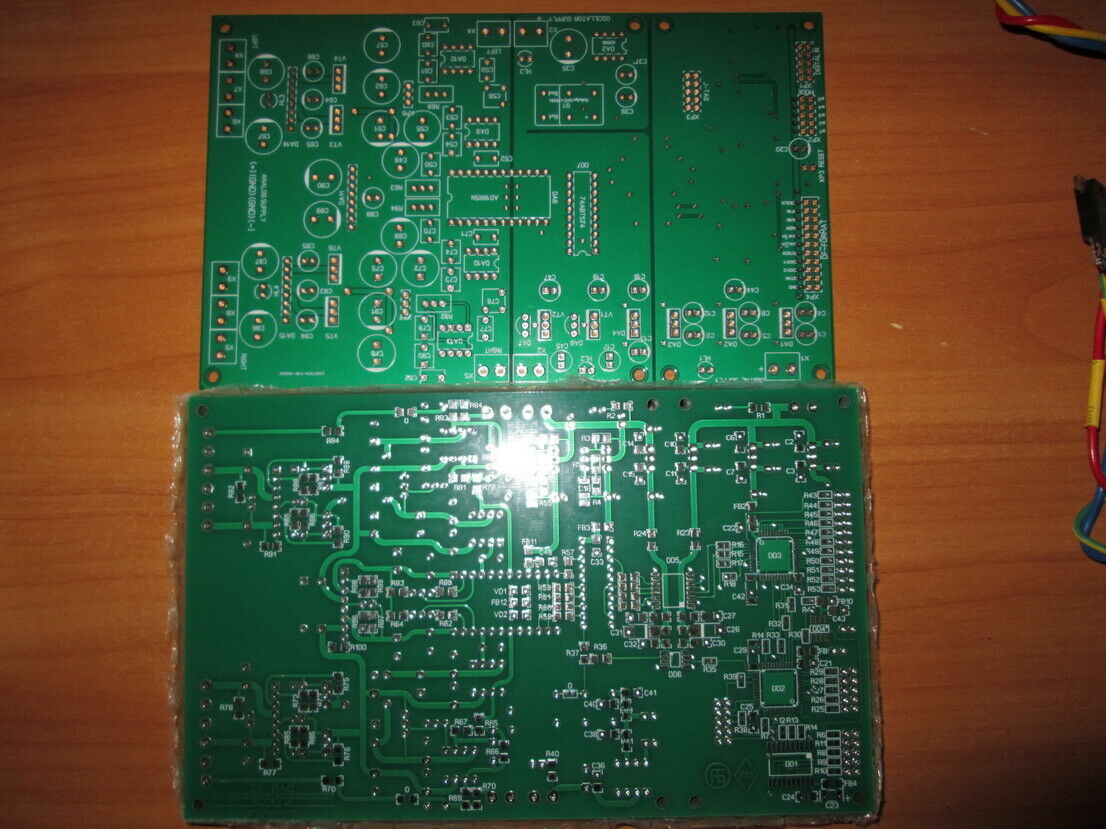
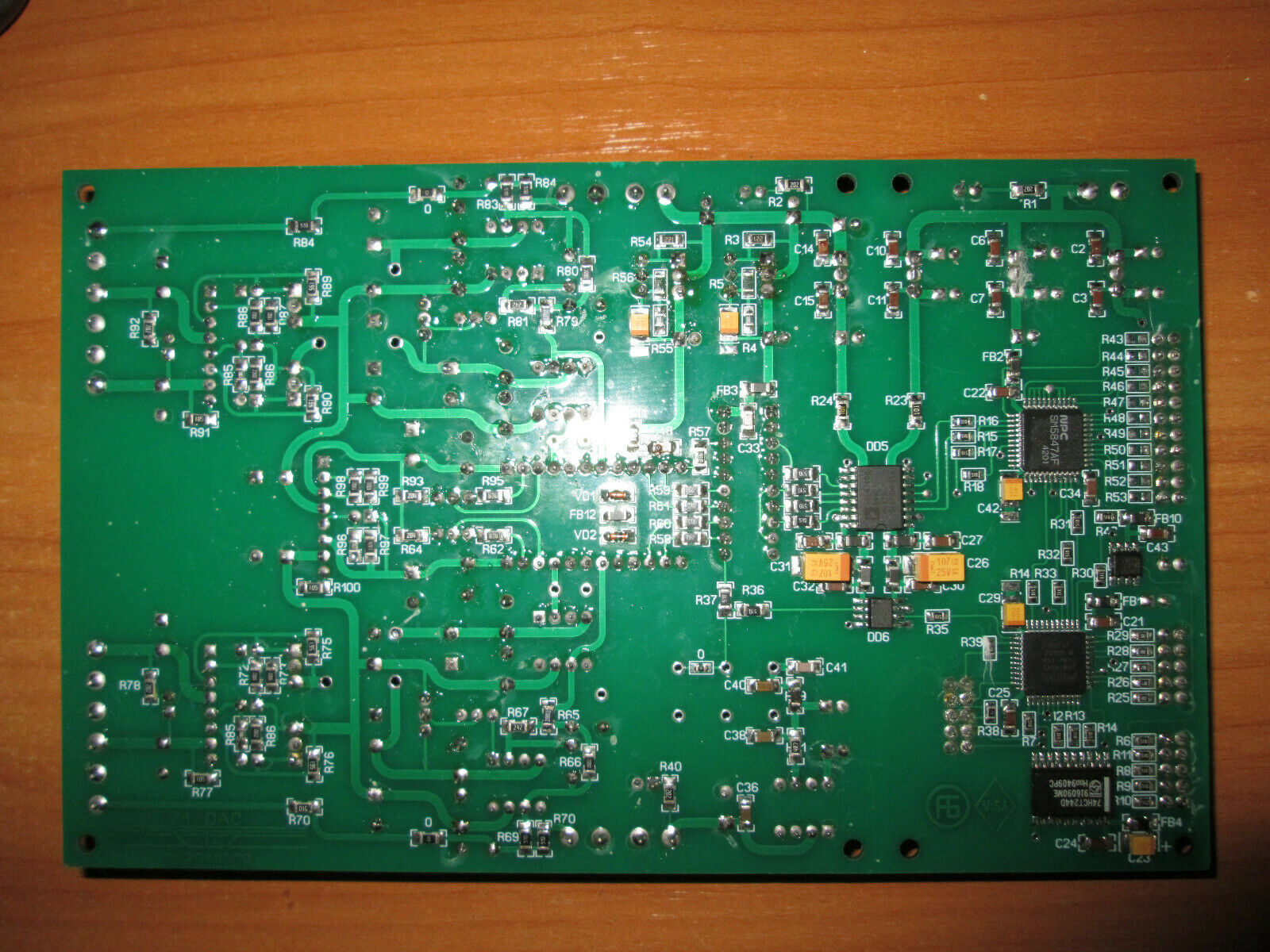
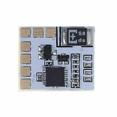
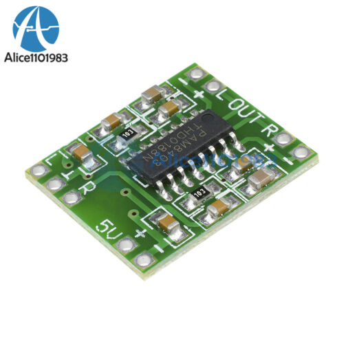
AD1865 DAC printed circuit board with programmed FPGA.
$ 25.87
- Description
- Size Guide
Description
DAC printed circuit board on AD1865 with programmed FPGA.The FPGA implements reference frequency dividers and an I2S Philips -> I2S RJ format converter.
The lot consists of one PCB and one FPGA chip. The last two photos are given as an example.
Jumper assignment on the board MODE block (XP2)
JP - ON - the jumper is installed (shorted);
JP - OFF - the jumper is removed (open);
1. JP5 (closest to the input connector) - data length for the shift I2S-> RJ;
JP5 - ON - 24 bit;
JP5 - OFF - 16 bit;
2. JP4 - input data format - I2S / RJ;
JP4 - OFF - I2S;
JP4 - ON - RJ;
3. JP3 - invert the input frequency of 768fs for FPGAs;
JP3 - ON - without inversion;
JP3 - OFF - with inversion;
4. JP2, JP1 - selection of the division coefficient K of the master block;
JP1 - ON, JP2 - ON - K = 3 (at the output of the DAC 256fs);
JP1 - ON, JP2 - OFF - K = 2 (at the output of the DAC 384fs);
JP1 - OFF, JP2 - ON - K = 1.5 (at the output of the DAC 512fs);
JP1 - OFF, JP2 - OFF - (at the output of the DAC 0fs);
